TPS7B4253QDDARQ1 SOIC-8 linear voltage regulator (LDO) cleaning inventory price beautiful
characteristic
Meet the requirements of automobile application
The following results are in accordance with AEC-Q100:
Device temperature level 1: ambient operating temperature range from - 40 ℃ to+125 ℃
Device Human Discharge Mode (HBM) Electrostatic Discharge (ESD) Classification Class 3A
Component charging mode (CDM) ESD classification level C6
– 40V to 45V wide input voltage range (maximum)
Adjustable output voltage range:
1.5V to 40V (HTSSOP)
2V to 40 V (SO PowerPAD)
300mA output current capacity
± 4mV ultra-low output tracking tolerance
320mV low voltage drop (when IOUT=200mA)
Separate pins for enable and trace inputs (HTSSOP only)
Low Quiescent Current (IQ):
<4 µ A (EN=low level)
Typical value is 60 µ A under light load
Ultra wide equivalent series resistance (ESR) range.
Stable when used with ceramic output capacitors in the range of 10 µ F to 500 µ F (ESR of 1m Ω to 20 Ω)
Reverse polarity protection
Current limiting and thermal shutdown protection
Output short circuit protection for grounding and power supply
Output pin inductive clamping
The following packages are available:
8-pin small form factor (SO) PowerPad package
20 pin heat dissipation thin small outline size (HTSSOP) package
application
Non onboard sensor power supply
High precision voltage tracking
Power switch for non board load
explain
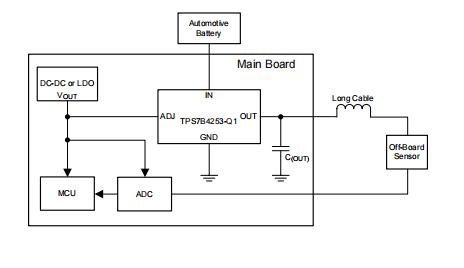
For automobile non onboard sensors and small current non onboard modules, the power supply is connected to the motherboard through a long cable. In such cases, the power supply device needs to provide protection for non board load to prevent board components from being damaged during battery short circuit caused by short circuit to ground or cable breakage. Non onboard sensors need to use the same power supply as onboard components to ensure high accuracy of data acquisition.
The TPS7B4253-Q1 device is designed for automotive applications with a 45V load drop problem. The device can be used as a low drop tracking (LDO) regulator or voltage tracker to build a closed power loop for non onboard sensors through the onboard main power supply. The output of the device is precisely regulated by the reference voltage of the ADJ pin.
In order to provide accurate power supply for non onboard modules, the device has an ultra-low tracking tolerance of 4mV between ADJ and FB pins within the operating temperature range. PMOS back-to-back topology eliminates the need for external diodes under reverse polarity conditions. TPS7B4253-Q1 device also includes thermal shutdown, inductive clamping, overload and battery short circuit protection to prevent on-board components from being damaged under extreme conditions.
Meet the requirements of automobile application
The following results are in accordance with AEC-Q100:
Device temperature level 1: ambient operating temperature range from - 40 ℃ to+125 ℃
Device Human Discharge Mode (HBM) Electrostatic Discharge (ESD) Classification Class 3A
Component charging mode (CDM) ESD classification level C6
– 40V to 45V wide input voltage range (maximum)
Adjustable output voltage range:
1.5V to 40V (HTSSOP)
2V to 40 V (SO PowerPAD)
300mA output current capacity
± 4mV ultra-low output tracking tolerance
320mV low voltage drop (when IOUT=200mA)
Separate pins for enable and trace inputs (HTSSOP only)
Low Quiescent Current (IQ):
<4 µ A (EN=low level)
Typical value is 60 µ A under light load
Ultra wide equivalent series resistance (ESR) range.
Stable when used with ceramic output capacitors in the range of 10 µ F to 500 µ F (ESR of 1m Ω to 20 Ω)
Reverse polarity protection
Current limiting and thermal shutdown protection
Output short circuit protection for grounding and power supply
Output pin inductive clamping
The following packages are available:
8-pin small form factor (SO) PowerPad package
20 pin heat dissipation thin small outline size (HTSSOP) package
application
Non onboard sensor power supply
High precision voltage tracking
Power switch for non board load
explain
For automobile non onboard sensors and small current non onboard modules, the power supply is connected to the motherboard through a long cable. In such cases, the power supply device needs to provide protection for non board load to prevent board components from being damaged during battery short circuit caused by short circuit to ground or cable breakage. Non onboard sensors need to use the same power supply as onboard components to ensure high accuracy of data acquisition.
The TPS7B4253-Q1 device is designed for automotive applications with a 45V load drop problem. The device can be used as a low drop tracking (LDO) regulator or voltage tracker to build a closed power loop for non onboard sensors through the onboard main power supply. The output of the device is precisely regulated by the reference voltage of the ADJ pin.
In order to provide accurate power supply for non onboard modules, the device has an ultra-low tracking tolerance of 4mV between ADJ and FB pins within the operating temperature range. PMOS back-to-back topology eliminates the need for external diodes under reverse polarity conditions. TPS7B4253-Q1 device also includes thermal shutdown, inductive clamping, overload and battery short circuit protection to prevent on-board components from being damaged under extreme conditions.
Schematic diagram of typical application circuit