ADS42LB49IRGCR analog-to-digital conversion chip ADC TI original stock
ADS42LB49 and ADS42LB69 are high linearity, dual channel, 14 and 16 bit 250MSPS mode converters (ADC) series that support DDR and QDR LVDS output interfaces. Buffered analog inputs provide a unified input impedance over a wide frequency range while greatly reducing sampling and maintaining the energy of spurious pulses. The sampling clock divider can achieve more flexible system clock architecture design.
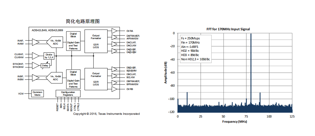
ADS42LBx9 provides excellent spurious free dynamic range (SFDR) over a wide input frequency range with low power consumption.
characteristic
• Dual channel
• 14 and 16 bit resolution
• Maximum clock rate: 250MSPS
Analog input buffer supporting high impedance input
• Support
Flexible input clock buffer for 1 division, 2 division, and 4 division
• 2VPP and 2.5VPP differential full scale input (SPI programmable)
• Double data rate (DDR) or Four Data Rate (QDR) Low Voltage Differential Signaling (LVDS) interface
64 pin ultra thin square flat leadless (VQFN) package (9mm × 9mm)
Power consumption: 820mW/channel
Gap jitter: 85 fs
Internal jitter
Channel isolation: 100dB
Performance at fIN=170MHz, 2 VPP, -1dBFS
Signal to Noise Ratio (SNR): 73.2dBFS
- No Stray Dynamic Range (SFDR):
– 87dBc (second harmonic (HD2) and third harmonic
(HD3)
– 100dBc (non HD2 and HD3)
• fIN=170MHz
Performance under 2.5 VPP, -1dBFS conditions:
- SNR: 74.9dBFS
- SFDR:
– 85dBc (HD2 and HD3)
– 97dBc (non HD2 and HD3)
application
• Communication and cable infrastructure
Multicarrier, multimode cellular receiver
• Radar and Smart antenna array
• Broadband wireless
• Testing and measuring instruments
• Software defined and diverse RF
• Microwave and dual channel I/O receivers
• Hub
• Power amplifier linearization