Tps22915cyfpr dsbga-4 power switch IC price advantage
explain
Tps22914 / 15 is a small, low Ron, single channel load switch with controlled slew rate. The device includes an N-channel metal oxide semiconductor field effect transistor (MOSFET), which can operate in the input voltage range of 1.05 V to 5.5 V and can support the maximum continuous current of 2A.
The switch is controlled by a switch input and can be directly connected to the low-voltage control signal. Small size and low Ron make this device very suitable for space limited and battery powered applications. The wide input voltage range of this switch makes it a multi-purpose solution for many different voltage rails. The controlled rise time of the device greatly reduces the inrush current caused by the high-capacity load capacitance, so as to reduce or eliminate the power consumption. By integrating a 143 Ω pull-down resistor for fast output discharge (QOD) when the switch is closed,
Tps22915 further reduces the overall solution size. Tps22914 / 15 adopts space saving small 0.78mm ×
4-pin wafer chip level (WCSP) package (YFP) with 0.78mm, 0.4mm spacing and 0.5mm height. The rated operating temperature range of the device in a naturally ventilated environment is – 40 ° C to + 105 ° C.
characteristic
• integrated single channel load switch
• input voltage range: 1.05 V to 5.5 V
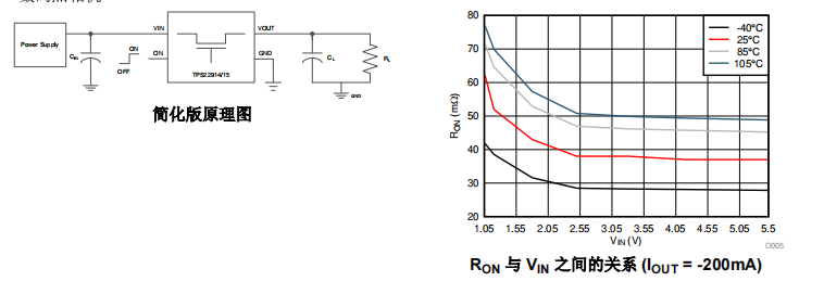
• low on resistance (RON)
– Ron = 37m Ω (typical at VIN = 5V)
– Ron = 38m Ω (typical at VIN = 3.3V)
– Ron = 43M Ω (typical at VIN = 1.8V)
• 2A maximum continuous switching current
• low quiescent current
– 7.7 µ a (typical at VIN = 3.3 V)
• a low control input threshold allows the use of a universal output voltage of 1 V or higher
Input output (GPIO) interface
• controlled conversion rate
– at VIN = 3.3V,
tR(TPS22914B/15B) = 64µs
– at VIN = 3.3V,
tR(TPS22914C/15C) = 913µs
• fast output discharge (only applicable to tps22915)
• subminiature wafer level chip size package
– 0.78mm × 0.78mm, 0.4mm spacing,
0.5mm height (YFP)
• electrostatic discharge (ESD) performance according to jesd 22 test
– 2KV human body discharge mode (HBM) and 1kV device charging model
(CDM)
application
• smart phones, mobile phones
• ultra thin, ultrabook ™/ Notebook computer
• Tablet PC, tablet phone
• wearable technology
• solid state drives
Tps22914 / 15 is a small, low Ron, single channel load switch with controlled slew rate. The device includes an N-channel metal oxide semiconductor field effect transistor (MOSFET), which can operate in the input voltage range of 1.05 V to 5.5 V and can support the maximum continuous current of 2A.
The switch is controlled by a switch input and can be directly connected to the low-voltage control signal. Small size and low Ron make this device very suitable for space limited and battery powered applications. The wide input voltage range of this switch makes it a multi-purpose solution for many different voltage rails. The controlled rise time of the device greatly reduces the inrush current caused by the high-capacity load capacitance, so as to reduce or eliminate the power consumption. By integrating a 143 Ω pull-down resistor for fast output discharge (QOD) when the switch is closed,
Tps22915 further reduces the overall solution size. Tps22914 / 15 adopts space saving small 0.78mm ×
4-pin wafer chip level (WCSP) package (YFP) with 0.78mm, 0.4mm spacing and 0.5mm height. The rated operating temperature range of the device in a naturally ventilated environment is – 40 ° C to + 105 ° C.
characteristic
• integrated single channel load switch
• input voltage range: 1.05 V to 5.5 V
• low on resistance (RON)
– Ron = 37m Ω (typical at VIN = 5V)
– Ron = 38m Ω (typical at VIN = 3.3V)
– Ron = 43M Ω (typical at VIN = 1.8V)
• 2A maximum continuous switching current
• low quiescent current
– 7.7 µ a (typical at VIN = 3.3 V)
• a low control input threshold allows the use of a universal output voltage of 1 V or higher
Input output (GPIO) interface
• controlled conversion rate
– at VIN = 3.3V,
tR(TPS22914B/15B) = 64µs
– at VIN = 3.3V,
tR(TPS22914C/15C) = 913µs
• fast output discharge (only applicable to tps22915)
• subminiature wafer level chip size package
– 0.78mm × 0.78mm, 0.4mm spacing,
0.5mm height (YFP)
• electrostatic discharge (ESD) performance according to jesd 22 test
– 2KV human body discharge mode (HBM) and 1kV device charging model
(CDM)
application
• smart phones, mobile phones
• ultra thin, ultrabook ™/ Notebook computer
• Tablet PC, tablet phone
• wearable technology
• solid state drives
• digital camera