Tle8108em pg-ssop-24 power switch IC advantages shipping
describe
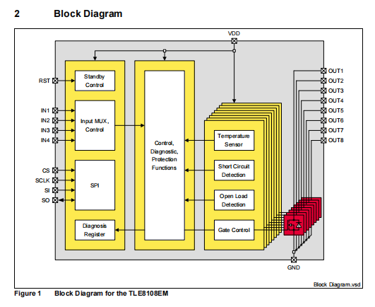
Tle8108em is an 8-channel low side switch in pg-ssop-24 package, which provides embedded protection function.
It is specially designed for powertrain automotive applications. Realize serial peripheral interface (SPI) to control and diagnose equipment and load. Four configurable direct inputs can be used to control the output in PWM. The device is single integrated. The internal switch is the power supply n-MOSFET.
Diagnostic feedback information
• lock diagnostic information through SPI register
• overtemperature detection (DOT)
• overload detection corresponds to battery short circuit (SCB) in the on state.
• open circuit load detection (OL) in disconnected state
• short circuit to ground detection (SCG) in off state
Protection function
• overload switch off
• overheat shutdown
• electrostatic discharge (ESD)
application
• resistive, inductive and capacitive loads
• designed for drive relays in automotive applications
General description
Tle8108em is an 8-channel low side relay switch, which is designed as a typical automotive relay and provides embedded protection function. Pg-ssop-24 package is used to obtain occupancy optimization solution. 16 bit serial peripheral interface (SPI) is used for equipment and load control and diagnosis. SPI interface provides daisy chain function.
The tle8108em is equipped with four input pins, which can be used to directly control its dedicated channels, thus providing flexibility in design and PCB layout. The input multiplexer is controlled by SPI.
The equipment provides a comprehensive diagnosis of the load, that is, open load, short circuit to ground and short circuit to battery detection. The SPI diagnostic bit indicates the possible latching fault condition.
Each output stage has short-circuit protection. In case of overload, the affected channel will be closed. Each channel has a temperature sensor, which can protect the equipment when the temperature is too high.
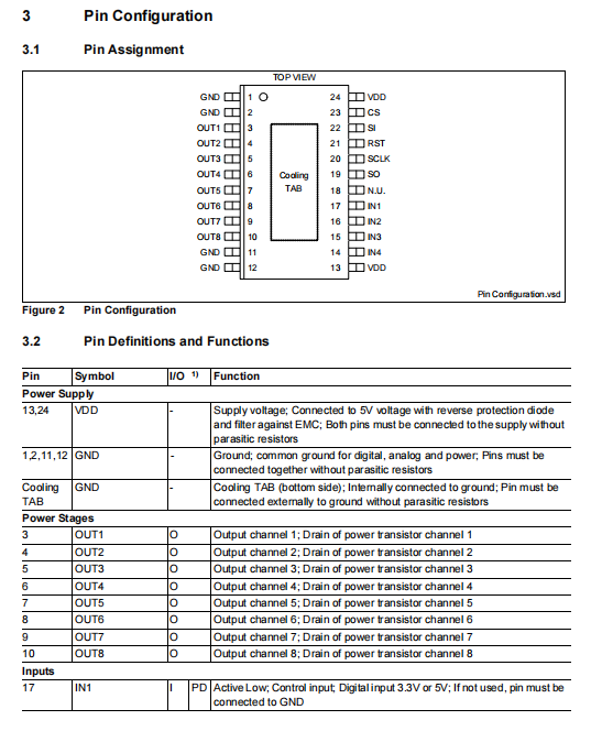
The equipment is powered by a single power supply. Its nominal working voltage is 5V.
The internal switch is the power supply n-MOSFET. The input is CMOS compatible with ground reference. The device is separately integrated into intelligent power technology.
All output pins are on one side of the device, while the other side binds the signal to the microcontroller, thereby promoting PCB layout.
Each channel can be set to clear mode (CLR) to clear the diagnostic flag; In the CLR state, the output is turned off and the diagnostic current is disabled.
Tle8108em is an 8-channel low side switch in pg-ssop-24 package, which provides embedded protection function.
It is specially designed for powertrain automotive applications. Realize serial peripheral interface (SPI) to control and diagnose equipment and load. Four configurable direct inputs can be used to control the output in PWM. The device is single integrated. The internal switch is the power supply n-MOSFET.
Diagnostic feedback information
• lock diagnostic information through SPI register
• overtemperature detection (DOT)
• overload detection corresponds to battery short circuit (SCB) in the on state.
• open circuit load detection (OL) in disconnected state
• short circuit to ground detection (SCG) in off state
Protection function
• overload switch off
• overheat shutdown
• electrostatic discharge (ESD)
application
• resistive, inductive and capacitive loads
• designed for drive relays in automotive applications
General description
Tle8108em is an 8-channel low side relay switch, which is designed as a typical automotive relay and provides embedded protection function. Pg-ssop-24 package is used to obtain occupancy optimization solution. 16 bit serial peripheral interface (SPI) is used for equipment and load control and diagnosis. SPI interface provides daisy chain function.
The tle8108em is equipped with four input pins, which can be used to directly control its dedicated channels, thus providing flexibility in design and PCB layout. The input multiplexer is controlled by SPI.
The equipment provides a comprehensive diagnosis of the load, that is, open load, short circuit to ground and short circuit to battery detection. The SPI diagnostic bit indicates the possible latching fault condition.
Each output stage has short-circuit protection. In case of overload, the affected channel will be closed. Each channel has a temperature sensor, which can protect the equipment when the temperature is too high.
The equipment is powered by a single power supply. Its nominal working voltage is 5V.
The internal switch is the power supply n-MOSFET. The input is CMOS compatible with ground reference. The device is separately integrated into intelligent power technology.
All output pins are on one side of the device, while the other side binds the signal to the microcontroller, thereby promoting PCB layout.
Each channel can be set to clear mode (CLR) to clear the diagnostic flag; In the CLR state, the output is turned off and the diagnostic current is disabled.
If all channels are set to CLR state, the standby mode (STB) of the device can be input; In STB mode, energy consumption is minimized.