Vsc8514xmk-14 qfn-138 Ethernet IC price advantage
Product Overview
The VSC8514-11 device is a low-power Gigabit Ethernet transceiver with copper media interfaces. It has
a low electromagnetic interference (EMI) line driver, and integrated line-side termination resistors that
conserve both power and printed circuit board (PCB) space.
The VSC8514-11 device includes Microsemi’s EcoEthernet™ 2.0 technology that supports Energy
Efficient Ethernet and power saving features to reduce power based on link state and cable reach.
The VSC8514-11 device uses Microsemi’s mixed signal and digital signal processing (DSP) architecture
to ensure robust performance even under less-than-favorable environmental conditions. It supports both
half-duplex and full-duplex 10BASE-T, 100BASE-TX, and 1000BASE-T communication speeds over
Category 5 (Cat5) unshielded twisted pair (UTP) cable at distances greater than 100 m, displaying
excellent tolerance to NEXT, FEXT, echo, and other types of ambient environmental and system
electronic noise.
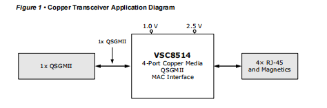
The following illustration shows a high-level, general view of a typical VSC8514-11 application.
Key Features
This section lists the main features and benefits of the VSC8514-11 device.1.1.1 Superior PHY and Interface Technology
• Four integrated 10/100/1000BASE-T Ethernet copper transceivers (IEEE 802.3ab-compliant)
with VeriPHY™ cable diagnostics
• QSGMII SerDes MAC interface
• Patented line driver with low EMI voltage mode and integrated line side termination resistors
• HP Auto-MDIX support and forced MDI/MDIX option
• Jumbo frame support up to 16 kB with programmable synchronization FIFOs
• IEEE 802.3bf register support for standardized access to information on data delay between the
MDI and xMII interface for a given PHY
1.1.2 Energy Efficiency
• EcoEthernet™ 2.0 green energy efficiency with ActiPHY™, PerfectReach™, and IEEE 802.3az
Energy Efficient Ethernet
• Fully optimized power consumption for all link speeds
• Integrated LED brightness control
• Clause 45 registers to support IEEE 802.3az Energy Efficient Ethernet and IEEE 802.3bf
1.1.3 Key Specifications
• 1.0 V and 2.5 V power supplies
• 3.3 V-tolerant 2.5 V inputs (single-ended and bi-directional TTL/CMOS I/Os)
• Compliant with IEEE 802.3 (10BASE-T, 100BASE-TX, and 1000BASE-T)
• QSGMII v1.3 and IEEE 1149.1 JTAG boundary scan
• Devices support operating temperatures of –40 °C ambient to 125 °C junction or 0 °C ambient to
125 °C junction
• Available in 12 mm x 12 mm, 138-pin, multi-row plastic QFN package